
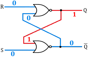
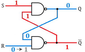
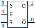
SR basic NOR gates Latches
The simplest latch circuit is the SR (Set, Reset) latch. It can store a single bit of information in the Q place and can hold its value
until a new input is performed, this is achieved by cross connecting the outputs of the NOR gates to the inputs of each other. The SR latch
can be constructed by two NOR or NAND gates. The NOR circuit is operated normally by two low inputs and need to apply high input (or 1) to
operate. Therefore, it is called active high. When the circuit is turned on, any of the values of Q or Q' can get the high value, it depends
only on the nature of the circuit, the first to get the signal will get the value of 1 and the other one the value of 0. at normal operation
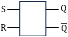
the last values of Q or Q' will apply. The symbol of this circuit is:
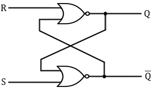
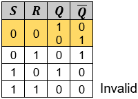
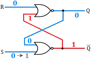
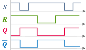
First startup
Both values of R and S are 0, we assume arbitrary that the latched bit Q value is 1.The symbol of this circuit is:
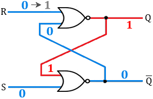
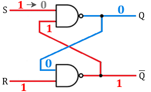
Press on the Reset button, now R=1
We have to check the new input with the last values of Q and Q' to verify if the new value of the latche will change.This will change the value of Q to 0, Q=0 and Q' to 1.
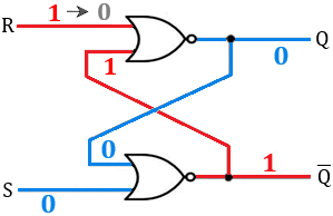
Reset R back to 0, R=0
This operation will cause no change in Q and it stays latched on 0.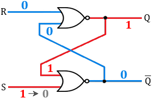
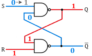
Pressing the Set button, now S=1
This operation will change the value stored in Q to 1, Q=1 and Q' to 0.
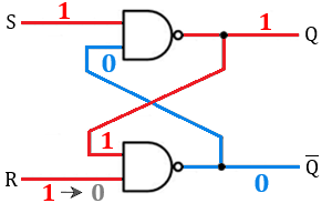
Pressing the Set button back to 0 S=0
This operation will cause no change in the latched value stored in Q and it remains equal to 1.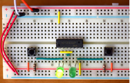
SR NOR Latch board assembly parts.
IC 7402 quad NOR gates.
2 light emitting diodes.
2 resistors 100 ohm.
2 on-off switches.
2 light emitting diodes.
2 resistors 100 ohm.
2 on-off switches.
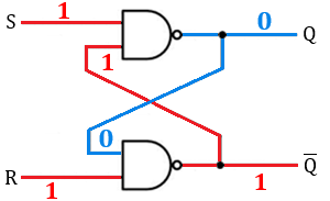
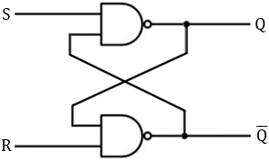
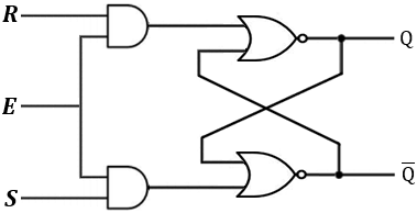
SR NAND gates Latch
The SR Latch can be made also from NAND gates. in this case the S and R buttons are in the opposite location,
basic state of this latch is high, it means that to set and reset it, we must apply low voltages, hence
it is considered as active low. The state of the outputs Q or Q' are depending on
the previous state of the circuit or randomly at the startup of the system. The general scheme of this circuit is:
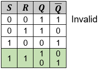
At startup S=1 and R=1. Q can be randomly set to 0 or 1 depend on the characteristics of the circuit.
The symbol of the NAND latch is:
Q is set to 0, Q = 0.
Q is changed to 1.
this causes no change in Q.
and the value of Q is changed to 0.
this will not cause any change in Q.
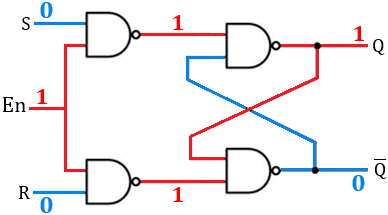
Simulation of SR NAND Latch with Enable button.
Error - Invalid
To improve the SR Latch, we can add an Enable button which is connected to additional 2 NAND gates. If Enable button is 0, then the system will
retain the last value of the Latch regardless of the inputs in S and R. However, the Enable button does not prevent the input of invalid
values in both inputs S=1 and R=1.
The system is active high, the normal state of the system is 0 and high pulse is required to change values.
The system is active high, the normal state of the system is 0 and high pulse is required to change values.
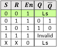
Ls - Last state.
SR NAND gate
The same results can be achieved by using an SR NOR gates, but this time we use another two AND gates.
Simulation of D-NAND Latch
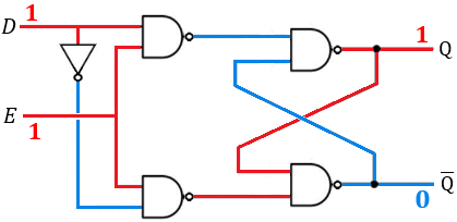
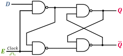
The possibility of illegal values can be eliminated by adding a NOT gate between the two inputs of 2 additional NAND gates.
this will prevent both values of Q and Q' not to get the value of 0 at the same time.
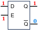
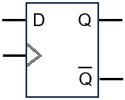
The letter D stands for Data input and the E letter stands for Enable input.
We can see that, while enable is high the Latched value in Q follows the value of the input D.
The letter D stands for Data input and the E letter stands for Enable input.
We can see that, while enable is high the Latched value in Q follows the value of the input D.
Simulation of improved D-NAND Latch
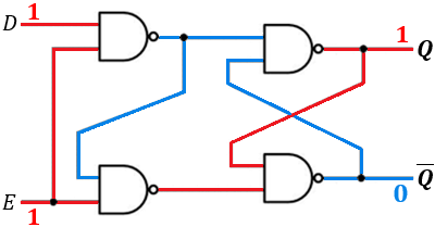
If we connect the output of the first NAND gate to the input of the second NAND gate, we get the same result, but
without the NOT gate, so the system is more efficient and less costly.
It is noticed that while enable E is high the stored Latch value Q, is following the value of the input D. When enable E is low the stored value of Q is locked on the last value regardless the value of D. This kind of circuit can use as a one-bit memory device.
It is noticed that while enable E is high the stored Latch value Q, is following the value of the input D. When enable E is low the stored value of Q is locked on the last value regardless the value of D. This kind of circuit can use as a one-bit memory device.
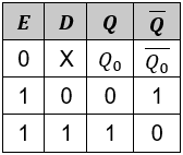
Q0 - Latches’ Last value
Clocked NAND D Latch
The D-latch is a one-bit memory device, we can connect several memory units to work together, but we should
synchronize all the D latches, this is done by connecting all the Enable inputs to a clock. A clock device will alternate
between 1 (high - 5 Volt) and 0 (low - 0 Volt) in a regular interval and forming a square wave. The cycle of the
pulse is measured by microseconds (μs).
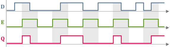
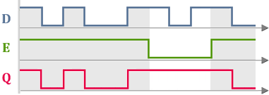
The Enable input, green square wave shape, is the clock pulses. Only during the high values of the clock, the latch value can be changed
otherwise it is locked to the last value of the latch.
D Latch Flip Flop

The D-latch is open to changes during half cycle of the clock (positive E) which can be several microseconds, this is a long time to except changes to the latch including unwanted data signals. To fix this problem we can limit the time that changes are possible to the time of the rising clock signal which are measured by nanoseconds and is described by the arrows in the drawing.
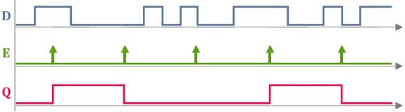
It is clear from the time diagram of the Flip Flop latch that the values of Q are slightly different then that of the previous clocked
D-Latch. This is because the input changes are ignored between consecutive rising edges.
D-Latch. This is because the input changes are ignored between consecutive rising edges.
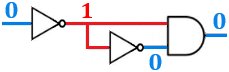
A simple rising edge detection device can be made from a NOT gate, connected to the input of an AND gate. It is because
the NOT gate has a certain delay measured in nanoseconds and hence the inputs to the AND gate for a very short instance will be 1 in both
inputs and the output of the AND gate will be 1, this short time is enough to update the latch. A longer delay time can be achieved by
adding odd number of NOT gates.

If we want to use the falling edge detector instead of the rising edge, we can add another NOT gate in the main input.
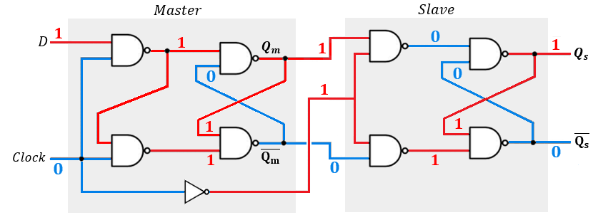
Master Slave D type Flip Flop
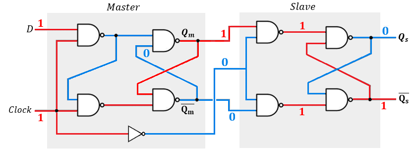
The Master Slave D type Flip Flop is assembled from a Gated D Latch (Master) whose outputs are connected to the inputs of a Gated SR
Latch (Slave) both are active high. A clock is connected to the Master and to the Slave via a NOT gate.
Notice that when the master Clock input is high and enables inputs to the Master, the Enable input of the Slave is low, hence input
to the Slave is disabled and waits to the clock to be low again to enable update to the slave Qs, at this time the Master is disabled.
This latch update process eliminates unwanted input signals to the Slave latch.
Time set diagram of Master Slave D type Flip Flop, when clock changed to 0
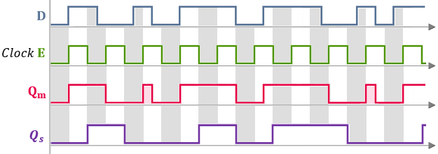
The Master is a simple Gated D Latch so the signal at Qm follows the signal of the input Data while E is positive (white strips) when E is
low or 0 (grey strips) the value of Qm is latched to the last value and the Slave gets the Qm value and updates the Qs latch.
It can be seen that the two unwanted glitches (pink background) that appears in the Qm time diagram are cancelled at the slave and has no affect on the Qs latch value.
It can be seen that the two unwanted glitches (pink background) that appears in the Qm time diagram are cancelled at the slave and has no affect on the Qs latch value.
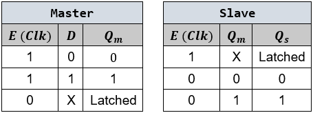
The true table of the Master and the Slave.
X − is any input value 0 or 1.
Latched − is the last value of Qm or Qs.
X − is any input value 0 or 1.
Latched − is the last value of Qm or Qs.