Gates implementation by transistors
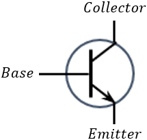
The use of a transistor as a logic gate, is based on the fact that a certain current in the base will allow the passing of
the current from the collector to the emitter (NPN transistor) and when the current in the base is near zero, the current between the collector
and the emitter is prevented. Therefore, the transistor is operating as a switch on – off device.

The transistor has 3 legs. The Base is the input and can represent 1 by applying generally 5V, in this case the current
will pass from the collector to the emitter (NPN transistor), or 0 by applying small voltage near zero, this will disable the passage of
current between the collector and emitter.
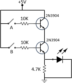
Implementation of AND gate

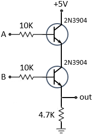
The AND gate is performed by two transistors connected as shown at left, note that the out current will be activated only
if A and B has current flow through them.
| AND gate truth table |
|---|
| A | B | Output | Symbol |
| 0 | 0 | 0 |  |
| 1 | 0 | 0 |
| 0 | 1 | 0 |
| 1 | 1 | 1 |
Implementation of OR gate

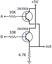
The connection of the transistors to achieve an OR gate is described in the left drawing. In this case both collectors are
connected to the current supply and both emitters are connected to the output.
| OR gate truth table |
|---|
| A | B | Output | Symbol |
| 0 | 0 | 0 |  |
| 1 | 0 | 1 |
| 0 | 1 | 1 |
| 1 | 1 | 1 |
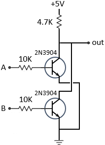
Implementation of NAND gate

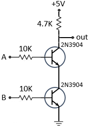
Notice that the only difference between AND and NAND gate is the connecting point of the output, while the connection of
out put in the AND gate is after the second emitter, the connection of the output of the NAND gate is before the first collector.
| NAND gate truth table |
|---|
| A | B | Output | Symbol |
| 0 | 0 | 1 |  |
| 1 | 0 | 1 |
| 0 | 1 | 1 |
| 1 | 1 | 0 |
Implementation of NOR gate

Notice that the only difference between OR and NOR gate is the connecting point of the output, while the connection of
out put in the OR gate is after the second emitter, the connection of the output of the NOR gate is before the first collector.
| NOR gate truth table |
|---|
| A | B | Output | Symbol |
| 0 | 0 | 1 |  |
| 1 | 0 | 0 |
| 0 | 1 | 0 |
| 1 | 1 | 0 |
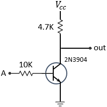
Implementation of NOT gate

The NOT gate is a very simple device and can be achieved by one transistor. Notice that when the input on the base is 0 no current
is flowing to the emitter hence all the current flow through the collector is provided to the output. And vice versa when the base
is on the current will floe through the emitter and reduce the current flow to the output and turning it to 0.
| NOT gate truth table |
|---|
| Input | Output | Symbol |
| 0 | 1 |  |
| 1 | 0 |
AND gate circuit experiment

The complete circuit of the AND gate is described in the drawing at left. We use as power supply 4 AA batteries to supply the input of 6V.
The complete circuit is assembled on a breadboard.

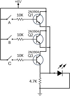
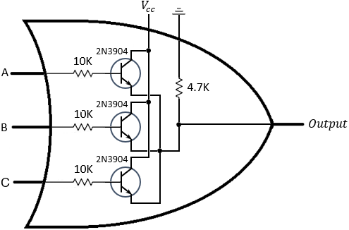
Triple input OR gate experiment

The circuit of 3 inputs OR gate is described in the drawing at left. We use as power supply 4 AA batteries to supply the input of 6V.
The complete circuit is assembled on a breadboard.

